Early on in the Crazyflie 2.0 design we decided on using a double-MCU architecture. The main reason for this was to add Bluetooth low energy (BLE) to the platform to permit new use-cases like controlling the Crazyflie 2.0 directly from a mobile device. It just so happens that Nordic semiconductor some time ago released a chip that perfectly matched our requirement: the nRF51822 can run a BLE stack and is still compatible with the nRF24Lx1 that we are using in the current Crazyflie and Crazyradio. This nRF51 chip contains an ARM Cortex-M0 microcontroller, powerful enough to implement the radio functionality and power management, but not powerful enough to run a fully featured Crazyflie. The resulting system architecture can be seen here:
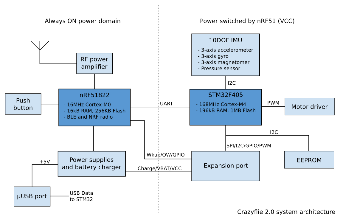
The nRF51822
The two main tasks for the nRF51 is to handle the radio communication and the power management. We use the radio for both CRTP and BLE, but the hardware also supports other protocols like ANT. The CRTP mode is compatible with the Crazyradio USB dongle and it provides a 2Mbit/seconds data link with low latency. Our initial tests of the Crazyflie 2.0 implementation shows that the latency of the radio link is between 360us and 1.26ms, at 2Mbps without retry and a packet size of respectively 1 and 32 bytes. The main benefit of the CRTP link with the Crazyradio is that it’s easily implemented on any system that supports USB host which, makes it the first choice to hack and experiment with the Crazyflie. To that we have added BLE, mostly with the use case of controlling the Crazyflie 2.0 from a mobile device. The idea is of course to be able to fly easily and on the go with BLE, but we also see lots of opportunities for fun hacks and experimentation with mobile devices. One idea we came up with is to be able to place the mobile device up-side-down on a table and to autonomously hover the Crazyflie above it using the camera on the back.
One of the other particularities of the nRF51 chip is that it was designed to run from a coin battery, which means that it is pretty well suited for low energy operation. So we decided to give the nRF51 the responsibility for power management as well. In the current version of the Crazyflie we have a small chip handling the ON/OFF button and cutting power to the complete board. On Crazyflie 2.0 the button is connected to one GPIO pin on the nRF51 and power to it will never be cut, it just goes in “power down” mode. This permits to reproduce the current ON/OFF functionality and the button can be used for more function like long press and double click. We have also added the possibility to wake up the system from one of the pins in the expansion connector, which allows wake-up by an external source. It also adds more possibilities like waking up the system at regular time-intervals to perform some function.
The STM32F405
We also updated the main MCU to a fast Cortex-M4 with a lot of memory. The CPU power is not a big limitation in the current Crazyflie, but the memory could become a limitation if users would like to implement new functionality that needs a lot more memory. We ran into this problem when we were trying to implement SD-card support for logging, as this required too big buffers. The new MCU has 196kB of RAM which should be enough for anyone (famous last words…). The MCU power will also allow for more computationally intensive algorithms, the first that comes in mind is sensor fusion between inertial sensors and the GPS data.
This amount of memory and computational power also open the doors for new things: the STM32F4 has a Memory Protection Unit, which allow to run tasks in a protected environment and intercept bugs before they can crash the full Crazyflie control firmware (like what happens on PC operating system). One use of this could be to to allow for “user code” that runs in a protected environment to allow easier development of advanced behavior. As always this kind of functionality spawns lots of crazy ideas :-) The leading one is to run a Lua interpreter in such a protected task. If there was a good API that could be used from Lua you could imagine lots of fun stuff to do. Like adding a new board with sensors, reading them and then controlling the Crazyflie from that, without having to go into the actual control algorithms or risking to crash the firmware. This is of course still a dream but at some point in the future we will definitely give it a try (when we have the time for it that is :-) ).
Inter-MCU communication
Working with a system with multiple MPU is hard. As embedded system developer we know that, so we designed the Crazyflie 2.0 with at least some idea of how to limit the problems related to debugging two inter-dependent MCUs. We have defined as precisely as possible the responsibility of each MCU, which permits to develop and test things independently:
- The nRF51 is responsible for
- ON/OFF logic
- Enabling power to the rest of the system (STM32, sensors and expansion board)
- Battery charging management and voltage measurement
- Master radio bootloader
- Radio and BLE communication
- Detect and check installed expansion boards
- The STM32 is responsible for all the rest, among other things:
- Sensor reading and motor control
- Flight control
- Telemetry (including the battery voltage)
- Additional user development
The nRF51 will act as slave and the STM32 as master. Using a radio bootloader it will be possible to wirelessly update the firmware for both MCUs.
We will write more details and post photos in the following weeks. Do not hesitate to tell us what you think about it, we appreciate all the feedback we get and we already have a couple of verification that we made after previous feedback (ie. radio latency and magnetometer usability).
Thanks Arnaud – that looks really cool! A few thoughts/questions on the design:
1.) Why did you decide to go with UART instead of SPI for Inter-MCU communication? I looked at the data sheets of both MCUs and it looks like the gcd for UART is 1 Mbit/s while SPI would run at 2 Mbit/s (both limited by the nRF51). Additionally, SPI has DMA support on the nRF51. If the nRF51 would be the SPI-Master it should be possible to get 4 Mbit/s.
2.) Will both chips be debuggable using JTAG?
3.) I think it would be useful to have some more pins from the nRF51 exposed at the expansion port as well. In case someone wants to add a third way of communicating or just some helper sensors for the crazyflie mesh you announced earlier, it would be really helpful to be able to extend the nRF51 directly, without going through the additional Inter-MCU communication.
4.) What is the use-case for the EEPROM? If its for fixed settings those could be baked into the firmware (or use an unused flash-block as fake-eeprom). Not that I don’t like it, but just as an idea in case it is expensive or complicated to route.
5.) What does “usb data to stm32” mean? Will it be possible to use the USB functionality of the STM32? I assume that would not include USB OTG?
6.) How would the nRF51 “Detect and check installed expansion boards”? Since the expansion port has connections to the STM32 and NRF51, it would be impossible for one of the chips to do the detection by itself.
7.) Which IMU do you have in mind? (I guess you will reveal that in an upcoming blog-post anyways:-)
8.) Which path do the latency measurements follow you provided? Is it PCCrazyradionRF51STM32, or just a subset of that? They seem to be really low to me, so they might not include the USB protocol overhead?
Thanks for the great write-up and for including the community! Can’t wait getting one of those:-)
Hi Wolfgang,
I will answer every point. I am adding a couple of points to our todo list to investigate some thing but no promises: we have already packed a lot in a pretty small space so some things might not be possible.
1. You are right the nRF51 is one of the only chip I know that can actually be a good SPI slave. This functionality is fairly recent (more recent than the first Crazyflie 2 design) so it was not in and it would be really hard to put it in now (actually the main problem comes from the PIN multiplexing of the stm32, it is really easy on the NRF side). Anyway more bandwidth would not be interesting: even with the radio at 2Mbps we cannot achieve 1Mbps of effective bandwidth. But this could permit to use the nRF51 unique UART for the expansion board which would be really interesting. We will look at it to see if it is possible to connect the nrf to STM SPI as well, however that looks hard.
2. Both will be debuggable and we are making a debug adapter board with an easy to use standard ARM-Jtag (20 and 10 pins). We have also connected and briefly tested the SWD port between CPUs (nRF SWD to STM SPI and vice-versa), for future master plans ;-).
3. As for now we have 3 pins on the expansion board for the nRF51: one for the Onewire memories and two others pretty much free. We can look at multiplexing some nRF and STM pins.
4. The idea of the EEPROM is to simplify the software: so that we don’t have to care about writing the flash and we dont stop the CPU doing so (the stm32F405 has only one flash bank). This is mostly something from the experience of the Crazyflie 1 that would have made our life easier.
5. The USB port is connected to the Stm32 OTG full speed port and the ID pin is connected, it is intended mostly as a USB peripheral. It also means that in theory OTG is possible but we do not have 5V supply for it (so USB host would require a cable that takes power somewhere else). OTG was not by design and we do not plan software for it yet but it came for free…
6. We plan to explain this in a future post but the theory is: we put 1-Wire memory on each expansion board. These memories are powered by the data bus (ie. nRF51) and addressed by a guaranteed unique chip ID. So even before powering VCC the nRF51 can detect and read these memories and so have the possibility of detecting bus conflict and chosing not to start VCC.
7. Invensense MPU9250
8. This is from the USB dongle starting to send the radio packet to the end of the UART communication to the STM (ie. when the STM have the data in memory). So yes you have to add 1ms for the USB.
Thanks for the inspiring comment.
/Arnaud
Thanks Arnaud for the detailed response. About #9: The MPU9250 has 9 axis (no pressure sensor). Do you plan to keep the MS5611 and connect it via I2C as before?
We still have an i2c pressure sensor. We are currently testing a ST sensor that looks promising, the LPS25H.
Hi Arnaud,
I had one question about the pressure sensors.
I’m not sure if this is sensitive information, but could you please share your thoughts on why you chose the LPS25H vs the MS5611?
You guys are doing amazing work with the Crazyflie!
Can’t wait for the 2.0!!
Not sure if you saw the announcement yet, but this could be interesting when it comes out:
https://www.nordicsemi.com/News/News-releases/Product-Related-News/LG-Innotek-develops-Bluetooth-Smart-module-that-carries-little-or-no-size-penalty-compared-to-a-discrete-solution-and-requires-no-RF-design-expertise-to-use
It should help to reduce the radio footprint and (presumably) the BOM cost. If it’s all that they say, it will make it almost trivial to add BLE / nRF24l01 to any design!
On a related note, have you published any source code for the Crazyflie 2.0 yet? I’m starting to work with the nRF51822, and am curious to see what you have so far.
Hi,
Yeah, that looks interesting! It’s great that the matching network is integrated.
We are planning on releasing the code when we release the Crazyflie 2.0.
The leading one is to run a Lua interpreter in such a protected task : +1
LuaJit : +10… although cortex M4 not supported yet…